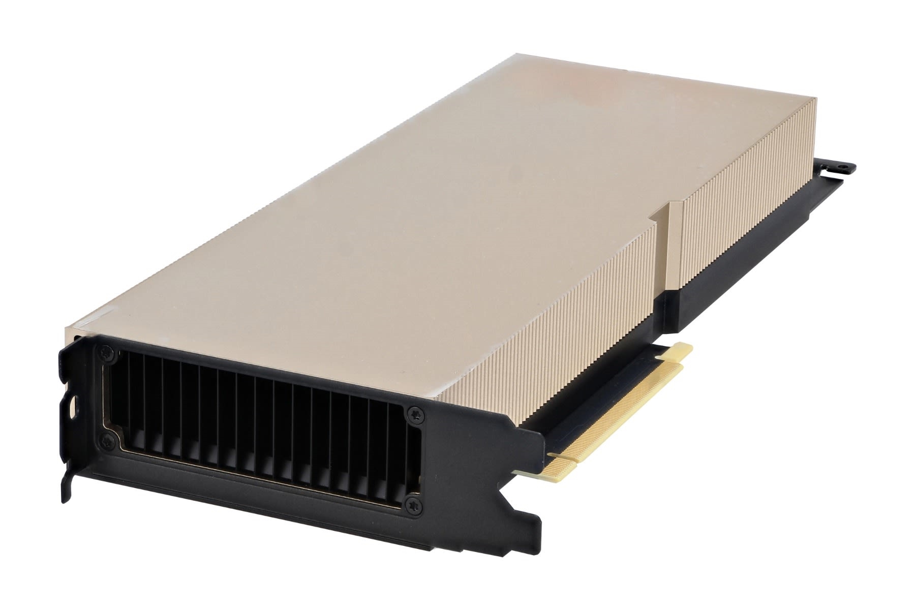
NVIDIA is bringing liquid-cooled GPUs to data centers
NVIDIA’s massive A100 GPU isn’t for you
Ampere’s long-awaited debut comes inside a $200,000 data center computer.

In this mini-episode of our explainer show, Upscaled, we break down NVIDIA’s latest GPU, the A100, and its new graphics architecture Ampere. Announced at the company’s long-delayed GTC conference, the A100 isn’t intended for gamers, or even for workstation users. Instead, it’s the direct replacement to the Volta-based V100 — a 2017 GPU purpose-built for data centers.
Volta never directly came to consumers — aside from the Titan V and a Quadro workstation card — but the improvements and tensor cores it introduced were a key part of Turing, the architecture which underpins almost all of NVIDIA’s current GeForce and Quadro cards. Whether the next generation of GeForce and Quadro cards are also called Ampere, or something else entirely, you can expect some of the A100’s new features to make their way over — and a lot of them not to.
NVIDIA was a little hazy on the finer details of Ampere, but what we do know is that the A100 GPU is huge. Its die size is 826 square millimeters, which is larger than both the V100 (815mm2) and the NVIDIA’s flagship gaming card, the RTX 2080 Ti (754mm2).
Those might not sound like big differences, but the A100 is NVIDIA’s first GPU to be built on TSMC’s 7nm process — its current models are on 12nm. That means there’s a roughly 40-percent reduction in the amount of space required for each transistor, which has let NVIDIA, apparently, squeeze 54 billion transistors into the A100. We say apparently because that’s such an enormous increase over, say, the 2080 Ti’s 18.6 billion transistors, that it almost feels like someone’s done their math wrong. With that said, some quick calculations put the A100’s transistor density at around 65 million per square mm, which is within the realms of possibility on TSMC’s 7nm process.
Moving away from transistors, the A100 has 6,912 FP32 CUDA cores, 3,456 FP64 CUDA cores and 422 Tensor cores. Compare that to the V100, which has 5,120 CUDA cores and 640 Tensor cores, and you can see just how much of an impact the new process has had in allowing NVIDIA to squeeze more components into a chip that’s only marginally larger than the one it replaces.
The A100 is being sold packaged in the DGX A100, a system with 8 A100s, a pair of 64-core AMD server chips, 1TB of RAM and 15TB of NVME storage, for a cool $200,000. For context, the DGX-1, a similar system with 8 V100s, cost around $150,000 at launch. That equates to a 33-percent generational price hike, but NVIDIA claims the A100 is 20 times faster at AI inference and training compared to the V100. And AI is really all these cards are likely to be used for — NVIDIA has already sold DGX A100s to partners in the space, and has sent one to the Argonne National Lab to aid in the fight against COVID-19.
This 20x performance jump is partially due to the massive increase in cores, but architectural improvements and new ways of doing math (which we dive into in our video) are likely contributing much more. The A100 is also helped by its memory: It has 40GB of HBM2 memory, compared to the 16GB the V100 launched with (the company bumped the memory on Volta cards to 32GB later), which means each DGX A100 system has 320GB of VRAM to play with.
So what can this tell us about NVIDIA’s much-anticipated new gaming cards? Well, concretely, some of these AI improvements will find their way into GeForce cards, improving performance in upscaling tasks like DLSS, or denoising, which is a key aspect of ray-tracing.
In a briefing with reporters, NVIDIA CEO Jensen Huang all-but-confirmed that, while there’s “great overlap in the architecture” between Ampere and the upcoming consumer cards, these gaming cards won’t feature HBM2 memory, and the sizing of the different elements in the chips will be very different, as they’ll be more focused on graphics performance than high-precision math. That means you should expect far higher gains in FP32 compute (which is where that TFLOP figure you hear about whenever a new GPU or console is launched comes from) for consumer cards, given so much of the A100’s die is given over to FP64-focused hardware.
Moving into theory crafting, a GeForce GPU the size of a 2080 Ti with a density approaching that of the A100, entirely targeted at gaming, would probably be twice as fast. To be clear, that’s highly unlikely to happen: NVIDIA will probably shrink the chip down considerably, reducing its costs and letting it sell much faster cards at similar prices to its current generation. The current rumor du jour comes from the YouTuber Moore’s Law is Dead, who suggests that the anticipated “3080 Ti” will have around 30-percent more cores than the 2080 Ti, which could make for a flagship GPU on a much-more reasonable 450mm2 die. Will a smaller die mean GPU prices go down? Given those specs will likely put NVIDIA’s offerings ahead of AMD’s rumored new cards, we doubt it.
(32)


