Nvidia Volta GV100 Unveiled at GTC 2017; Includes 5120 CUDA Cores, 16 GB HBM2, and 12nm FinFET Process
GTC 2017 today saw an incredible launch when Nvidia announced it beast – Nvidia Volta GV100. This next generation GPU is the first in the industry to make use of TSMC 12nm FinFET process. Designed for AI deep learning, there is probably no other GPU that can compare to this piece of tech.
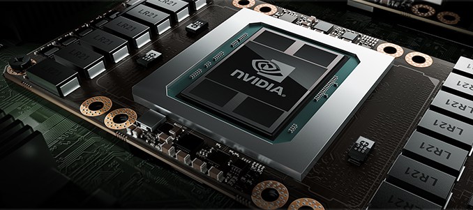
Nvidia has announced this chip as the successor to the GP100 GPU that was based on Pascal and was announced last year at GTC. It was the fastest graphics chip made for supercomputers then. With the GV100 and all the new tech involved, the company is taking the graphics performance ahead by leaps and bounds.
Compared to its predecessor, the Volta based GV100 is significantly better and that’s because of the processing power it holds inside. The GPU comes with 41 TPCs which each having two Volta streaming multiprocessor units. Each of the 84 SMs has 64 CUDA cores that totals to 5376 CUDA cores.
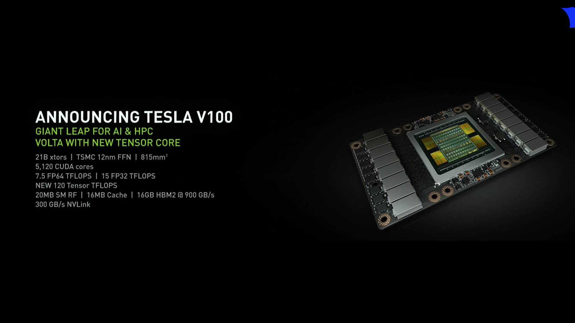
With a die size of 815mm2, the GPU has 21.1 billion transistors. Its power efficiency also gets improved and as a result, GV100 offers better performance per watt when compared to its predecessor.
The memory architecture has also seen an update and it now comes with eight 512-bit memory controllers. Its 4096-bit bus interface supports up to 16GB of HBM2 VRAM. The transfer rate has also increased to 900 GB/s from 720 GB/s on the GP100 using the increased speed of 900 MHz. Total 6MB of L2 cache is available for the entire chip with each memory controller having 768KB of L2 cache. It has a TDP rated at 300W.
With the use of new Tensor Cores, the Volta GV100 will be able to reach the level of performance that is required for training large neural networks. These cores deliver up to 120nTensor TFLOPS which is 12x higher peak TFLOPS on Tesla V100 for deep learning training compared to P100 FP32 operations. There are 8 Tensor Cores per SM making a total of 640 for the GPU.
Many of the newer versions of the deep learning frameworks will be able to use the performance level offered by Volta for higher multi-node training performance and training times. Not only deep learning, the higher performance of the Volta GV100 can also be leveraged for high performing computing (HPC) applications. New APIs and support for Volta features has been included in the Nvidia CUDA Toolkit version 9.0.
The post Nvidia Volta GV100 Unveiled at GTC 2017; Includes 5120 CUDA Cores, 16 GB HBM2, and 12nm FinFET Process appeared first on MobiPicker.
(116)